(China (Mainland))


Product Summary
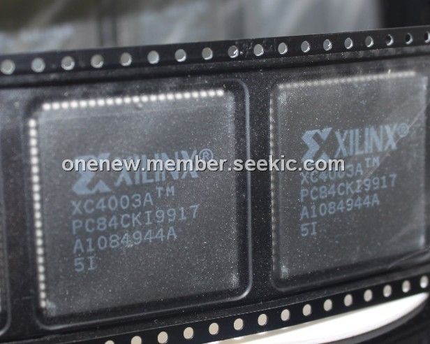
The XC4003A-5PC84I Field-Programmable Gate Array (FPGA) provides the benefits of custom CMOS VLSI, while avoiding the initial cost, time delay, and inherent risk of a conventional masked gate array. The XC4003A-5PC84I provides a regular, flexible, programmable architecture of Configurable Logic Blocks (CLBs), interconnected by a powerful hierarchy of versatile routing resources, and surrounded by a perimeter of programmable Input/Output Blocks (IOBs). The XC4003A-5PC84I has generous routing resources to accommodate the most complex interconnect patterns. The XC4003A-5PC84I has reduced sets of routing resources, sufficient for their smaller size. XC4000H high I/O devices maintain the same routing resources and CLB structure as the XC4003A-5PC84I, while nearly doubling the available I/O.
Parametrics
XC4003A-5PC84I absolute maximum ratings: (1)VCC Supply voltage relative to GND Commercial 0℃ to 85℃ junction: 4.75 to 5.25 V; (2)VIH High-level input voltage (XC4000 has TTL-like input thresholds): 2.0 to VCC V; (3)VIL Low-level input voltage (XC4000 has TTL-like input thresholds): 0 to 0.8 V; (4)TIN Input signal transition time: 250 ns.
Features
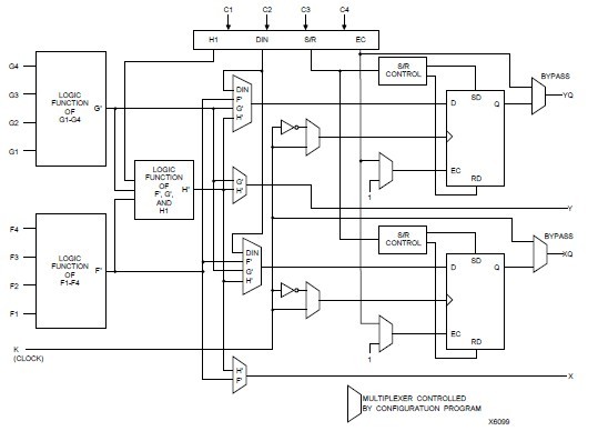
XC4003A-5PC84I features: (1)Abundant flip-flops; (2)Flexible function generators; (3)On-chip ultra-fast RAM; (4)Dedicated high-speed carry-propagation circuit; (5)Wide edge decoders; (6)Hierarchy of interconnect lines; (7)Internal 3-state bus capability; (8)Eight global low-skew clock or signal distribution network.
Diagrams
 |
 XC4000 |
Other |
|
Data Sheet |
Negotiable |
|
||||
|
XC4000A |
Other |
|
Data Sheet |
Negotiable |
|
||||
|
XC4000E |
Other |
|
Data Sheet |
Negotiable |
|
||||
|
XC4000H |
Other |
|
Data Sheet |
Negotiable |
|
||||
|
XC4000X |
Other |
|
Data Sheet |
Negotiable |
|
||||
|
XC4000XL |
Other |
|
Data Sheet |
Negotiable |
|
||||